







- Stock: In Stock
- Model: UTD2101E PLUS
- Weight: 3.00kg
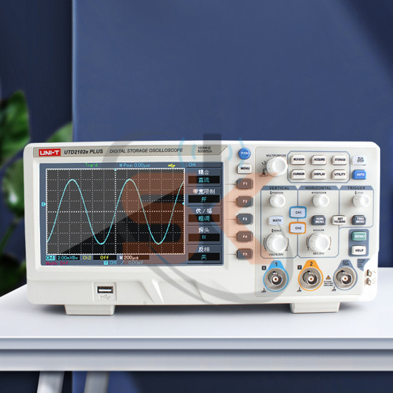
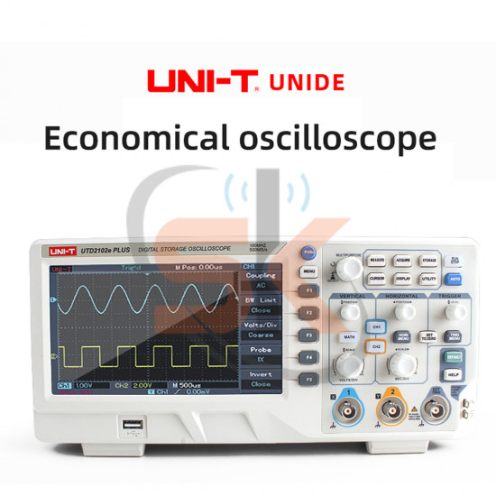
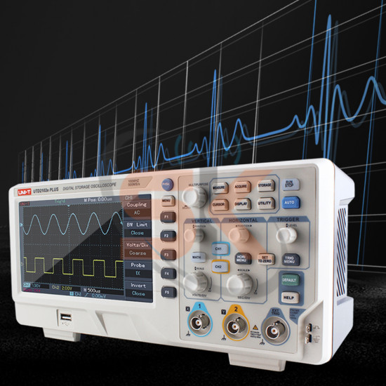
The UNI-T UTD2102E PLUS Digital Storage Oscilloscope is a professional-grade 100MHz benchtop test and measurement instrument engineered for electronics design laboratories, mobile motherboard diagnostic stations, and chip-level micro-soldering benches. Built to bridge the diagnostic gap that standard multimeters cannot solve, this 2-channel oscilloscope allows technicians to visualize transient signals, verify clock oscillations, detect high-frequency switching noise on PMIC buck rails, and decode serial communication protocols such as I2C, SPI, and UART in real time.
Equipped with a vivid 7-inch widescreen WVGA color TFT display, a real-time sampling rate of 500 MS/s (up to 1 GS/s peak equivalent), and deep waveform memory storage, the UTD2102E PLUS captures fast-rising pulse edges and sporadic glitches effortlessly. Its plug-and-play USB host/device interface and multi-trigger capabilities ensure fast, accurate root-cause identification for complex smartphone fault conditions such as bootloops, dead clock crystals, missing display PWM feeds, and baseband communication dropouts.
Key Engineering Features & Bench Advantages:
- Dual-Channel 100MHz Bandwidth: Offers two fully independent analog channels with low vertical noise floor, providing the bandwidth needed to inspect crystal oscillator frequencies (e.g., 19.2MHz, 24MHz, 38.4MHz baseband clocks) and fast signal edges on phone logic boards.
- High-Speed Real-Time Sampling: Delivers up to 500 MS/s real-time acquisition (with high-density equivalent time sampling), preventing waveform aliasing and ensuring transient spikes and voltage dips are captured accurately.
- 7-Inch Widescreen Color TFT Display: Features an 800×480 WVGA high-resolution screen with clear 8×16 division grid scaling, making it easy to analyze dual-channel overlaid signals, zoom into packet headers, and view on-screen measurement markers.
- Comprehensive Automated Measurement Suite: Supports over 30 automatic parameter measurements (including Vpp, Vmax, Vmin, Frequency, Period, Rise/Fall Time, Duty Cycle, and Phase) alongside on-screen cursor tracking.
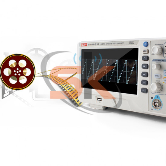
- Versatile Triggering Architecture: Includes Edge, Pulse Width, Slope, and Video trigger modes with adjustable trigger sensitivity and noise-rejection filters to lock onto complex modulated signals.
- Direct USB Connectivity & PC Storage: Front-panel USB host port supports quick one-touch saving of waveform screenshots and CSV data to flash drives, while the rear USB device port connects to PC software for continuous data logging and analysis.
- Built-in Hardware Frequency Counter: Integrated 6-digit real-time frequency counter provides instant readout of oscillator frequencies without requiring manual cursor calculations.
Technical Specification Matrix
Parameter Profile | Product Specification Details |
Product Model | UNI-T UTD2102E PLUS (UTD2000 Series) |
Bandwidth | 100 MHz |
Analog Channels | 2 Independent BNC Channels |
Real-Time Sampling Rate | 500 MS/s (Half Channel) / Standard Dual-Channel Real-Time Capture |
Rise Time | $\le 3.5\text{ ns}$ |
Memory Depth | Up to 64 kpts per channel |
Vertical Sensitivity | 1 mV/div – 20 V/div |
Timebase Scale | 2 ns/div – 50 s/div |
Trigger Types | Edge, Pulse Width, Slope, Video, Alternate |
Display Panel | 7.0-Inch TFT LCD, 800 × 480 WVGA Resolution |
Interface Ports | USB Host (Front), USB Device (Rear), Pass/Fail BNC Out |
Primary Bench Applications | Mobile Logic Board Diagnostics, Clock Crystal Verification, I2C/SPI Signal Tracing, PMIC Buck Converter Waveform Testing |
Practical Mobile Motherboard Diagnostic Guide:
- Probe Compensation Check: Connect the oscilloscope probe to Channel 1, clip the ground alligator lead to the probe ground ring, and connect the probe tip to the 1kHz square-wave calibration lug on the front panel. Adjust the probe compensation trimmer until the displayed square wave exhibits crisp 90-degree corners with no overshoot or undershoot.
- Clock Crystal Testing (Sleep & Baseband Clocks): Ground your probe to a solid motherboard shielding frame ground. Set Channel 1 coupling to AC and bandwidth limit to 20MHz (if testing a 32.768kHz sleep crystal). Power on the logic board and touch the probe tip to the crystal output terminal to confirm sinusoidal oscillation, peak-to-peak amplitude, and stable frequency output on the counter.
- PMIC Buck Rail Noise & Ripple: Switch coupling to AC, adjust vertical scale to 10mV/div or 20mV/div, and probe the output inductors around the main Power Management IC (PMIC). A healthy buck regulator shows a clean triangular ripple; excessive spikes, ringing, or erratic collapse points indicate degraded filter capacitors or damaged silicon.
- I2C & Serial Bus Diagnostics: Set trigger mode to Edge (falling or rising edge of the SCL clock line). Probe the SDA (Data) line on Channel 2 to view transmission packets. Use single-shot trigger mode to capture rapid initialization communication bursts during device power-up cycles to detect stuck bus lines.


-250x250h.jpg "2UUL PC01 Power Max 200W Multi-Port Charger Adjustable Voltage Integrated Power Supply")