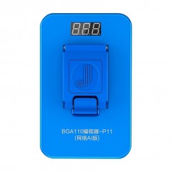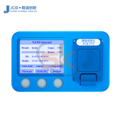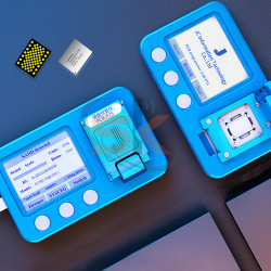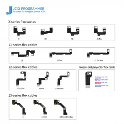



The JCID V1S Pro BGA70 NAND Programmer Module is an engineering-grade read, write, and repair socket module engineered for chip-level micro-soldering technicians, logic board diagnostic labs, and mobile refurbishment workshops. Serving as a dedicated expansion dock for the flagship JCID V1S Pro programmer, this specialized module enables deep-level access to Apple PCIe BGA70 NAND flash memory used across legacy and volume-repair iPhone and iPad models.
Designed to resolve stubborn motherboard faults—such as NAND corruption, NAND-related iTunes restore errors (Error 9, Error 4013, Error 4014), boot-loop cycling, and Wi-Fi hardware mismatch locks—this module also functions as the bench standard for lucrative storage capacity upgrades (e.g., upgrading 16GB/32GB/64GB devices to 128GB or 256GB). Engineered with a zero-insertion-force clam-shell bed and industrial gold-plated pogo pins, it allows direct read/write operations without requiring pre-tinning or damaging fragile solder pads.
Key Engineering Features & Bench Advantages:
- SYSCFG Data Read / Write / Backup: Read, write, back up, and modify complete factory System Configuration (SYSCFG) data, including device Serial Number, Model/Area codes, Bluetooth MAC, Wi-Fi MAC, and factory calibration tables.
- One-Click Wi-Fi Unbind: Instantly unbinds encrypted Wi-Fi data from the NAND SYSCFG sector, allowing technicians to replace malfunctioning Wi-Fi ICs directly without desoldering or replacing the CPU and EEPROM.
- Storage Capacity Expansion: Supports full formatting, repartitioning, and SYSCFG flashing on donor or new BGA70 PCIe NAND chips to execute memory upgrades on iPhone 6S–7 Plus and iPad models.
- Zero-Damage Clam-Shell Test Socket: Features high-durability, spring-loaded gold contact pins within an alignment-molded socket bed, ensuring rapid, reliable data transmission while eliminating mechanical wear on raw NAND pads.
- Dual Operation Flexibility: Supports standalone operation directly through the V1S Pro touchscreen interface as well as advanced partition editing and automated cloud backup when connected to the JCID Repair Assistant PC software suite.
- PCIe Error Code Rectification: Formats corrupted partition structures to resolve persistent storage-related iTunes restore errors, including Error 9, Error 14, Error 2009, Error 4013, and Error 4014.
Technical Specification Matrix
Parameter Profile | Product Specification Details |
Brand / Tool Platform | JCID / Designed Exclusively for JCID V1S Pro Host |
Supported Socket Architecture | BGA70 PCIe NAND Flash Memory (70-Ball Grid Array) |
Compatible iPhone Models | iPhone SE (1st Gen), iPhone 6S, iPhone 6S Plus, iPhone 7, iPhone 7 Plus |
Compatible iPad Models | iPad 5 (2017), iPad 6 (2018), iPad 7 (2019), iPad Pro 9.7, iPad Pro 10.5, iPad Pro 12.9 (Gen 1 & 2) |
Functional Capabilities | Read, Write, Format, SYSCFG Modification, Wi-Fi Unbind, Storage Partitioning |
Interface / Mounting | Gold-Plated Direct Header Interface (V1S Pro Expansion Bay) |
Software Support | On-Device V1S Pro Touch OS & JCID Repair Assistant PC Suite |
Primary Bench Utility | Memory Upgrades, Wi-Fi Unbind, iTunes Error Repair, Board Restoration |
Recommended Bench Operation Guide:
- Module Docking: Power down or place the JCID V1S Pro in standby mode. Align the BGA70 module with the secondary expansion slot on the host programmer and press gently until the gold-plated connector header seats firmly.
- NAND Extraction & Pad Cleanup: Desolder the target BGA70 NAND chip from the logic board using hot air set to 340°C–350°C with appropriate nozzle shielding. Clean all underfill and residual solder from the chip's pads using a soldering iron with desoldering braid and high-purity PCB cleaner until the pads are completely flat and shiny.
- Socket Insertion: Release the clam-shell latch on the BGA70 module. Align Pin 1 on the NAND chip with the alignment dot indicated inside the socket tray, set the chip flat onto the contact pins, and clamp the latch shut.
- Data Read & Backup: Select the "BGA70 NAND" application on the V1S Pro touchscreen (or within the JCID Repair Assistant PC software). Click Read to extract the device's SYSCFG information and save a backup copy locally.
- Modification / Upgrade:
- For Wi-Fi repair: Click Unbind Wi-Fi to clear the encryption lock from the data string.
- For storage upgrades: Insert the upgraded capacity blank or donor NAND, execute Format, and write the backed-up SYSCFG parameters back into the flash partition.
- Reballing & Board Installation: Reball the NAND using an appropriate 0.12mm BGA70 stencil and 183°C leaded solder paste. Re-solder the chip to the motherboard at 330°C–345°C, allow the board to cool naturally, and perform a full DFU restore via 3uTools or iTunes.